Language Plugin for schematic files of GSchem
Introduction
The plan [1] is to write a plugin for Gnucap to support schematic files from gEDA/gschem [2].
Schematics are graphical representation of circuits using abstract symbols showing components and their connections.
The idea for netlist import and export is at the wiki page : Netlist import and export
The technical details on on how this gEDA/gschem plugin is implemented is at the page: Details of gEDA plugin
How to parse schematics
The schematic files are converted into verilog netlist. The steps involved in parsing the schematic are described below, as observed by working out a few examples manually :
Identifying components
- Search for the identifier “C” at the start of the line.
- Search for the device name of the component. If device=none or graphical=1 (in the symbol file of the component), then ignore it as it doesn't have any electrical significance [3]. Else, index them in the order of their occurrence in the schematic.
- Get the name and value of the attributes associated with the components recognized by index of the component.
Positioning the nodes and pins
- Get the components' placement information from the schematic and using the placement of the components and the relative position of pins from the symbol file of the component, get the positions of active edges of the pins of all the components.
- For each component, get the pins' active edge's relative coordinates are in the symbol file say (px,py).Then execute the logic as shown below to get the position of the pins. (Say component position is (cx,cy))
- Create a `ifdef directive to write the placement of nodes in it. Nodes are placed at the corresponding pins from which they originate. 'place' in verilog has attributes x,y corresponding to x-coordinate and y-coordinate of the nodes' placement.
     if mirror_flag==0:
       if angle==0:
         (pxn,pyn)=(cx,cy) + (+px,+py)
       elif angle==90:
         (pxn,pyn)=(cx,cy) + (-py,+px)
       elif angle==180:
         (pxn,pyn)=(cx,cy) + (-px,-py)
       elif angle==270:
         (pxn,pyn)=(cx,cy) + (+py,-px)
     elif mirror_flag=1:
       if angle==0:
         (pxn,pyn)=(cx,cy) + (-px,+py)
       elif angle==90:
         (pxn,pyn)=(cx,cy) + (-py,-px)
       elif angle==180:
         (pxn,pyn)=(cx,cy) + (+px,-py)
       elif angle==270:
         (pxn,pyn)=(cx,cy) + (+py,+px)
Writing nets between pins
- Search for nets in schematics identified by “N” at start of line.
- For each net get the two co-ordinates it is connecting. If there are already nodes at those co-ordinates, create a net with those nodes as endpoints. Else create some name for the new node and save the node.
- Check the placement of the nodes to see if any nodes are implicitly connected, i.e, if they have same co-ordinates. If True, create a net between them
- Go through all nets and check all the nodes(except those the net ends in), if they are on that net. If True, create a net from the node to one of the end-nodes of the net.
- Complex nets can be simplified but don't need to be. If done, resulting schematic from this netlist on re-conversion differs.
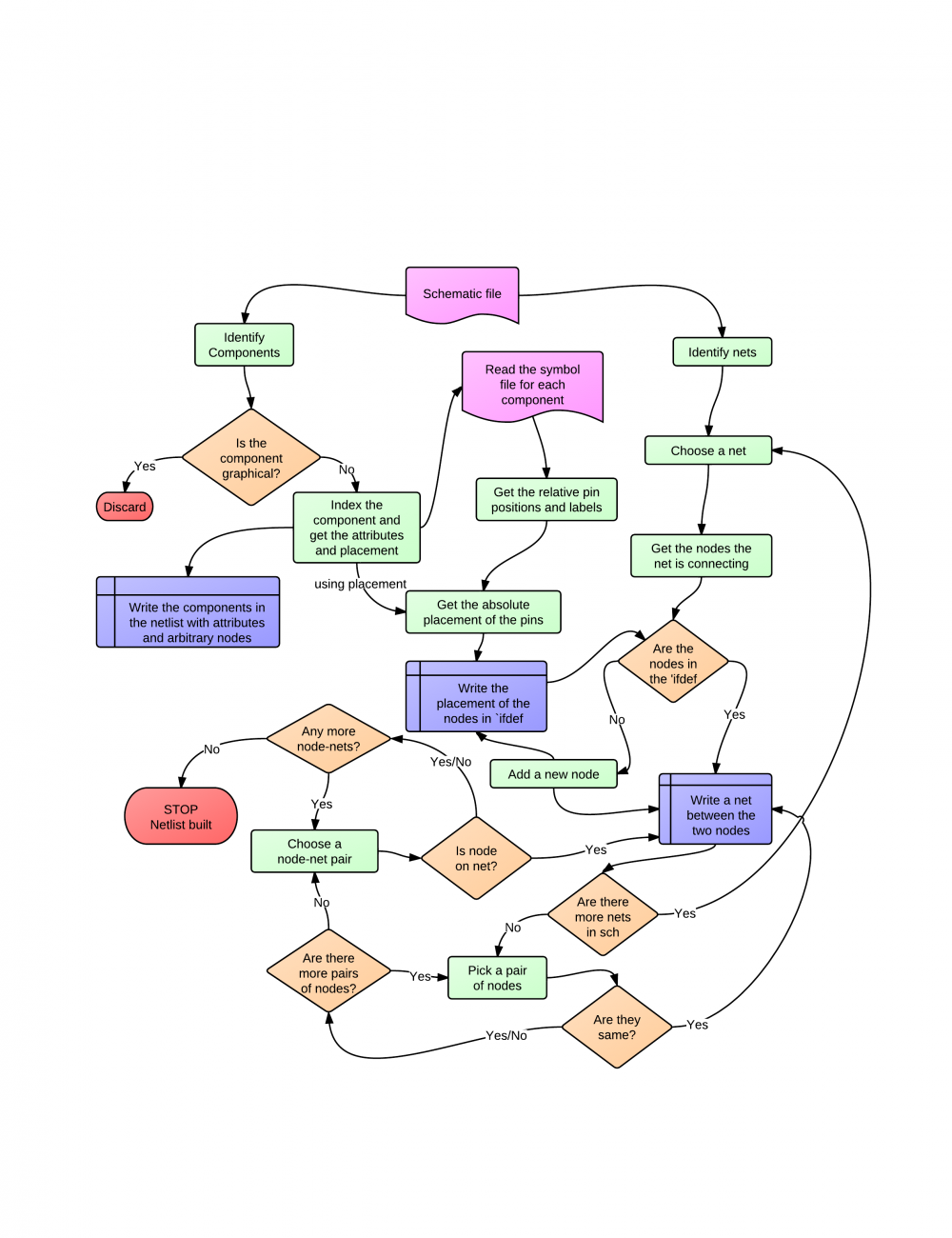
The Flow Chart for parsing the schematic is as follows :

Example of parsing:1
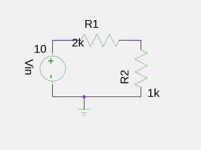
Consider the voltage divider circuit as shown below :
 It's schematic voltage_divider.sch is :
v 20100214 2
C 40000 40000 0 0 0 title-B.sym
C 44000 49000 1 90 1 voltage-3.sym
{
T 43300 48800 5 8 0 0 270 2 1
device=VOLTAGE_SOURCE
T 43500 48700 5 10 1 1 270 2 1
refdes=Vin
T 43500 48800 5 10 1 1 0 0 1
value=10
}
C 44100 48900 1 0 0 resistor-1.sym
{
T 44400 49300 5 10 0 0 0 0 1
device=RESISTOR
T 44300 49200 5 10 1 1 0 0 1
refdes=R1
T 44100 48900 5 10 1 1 0 0 1
value=2k
}
C 45300 48100 1 90 0 resistor-1.sym
{
T 44900 48400 5 10 0 0 90 0 1
device=RESISTOR
T 45000 48300 5 10 1 1 90 0 1
refdes=R2
T 45300 48100 5 10 1 1 0 0 1
value=1k
}
N 43800 48100 45200 48100 4
C 44200 47800 1 0 0 gnd-1.sym
N 43800 49000 44100 49000 5
N 45000 49000 45200 49000 6
- When parsing this, we convert it into an augmented netlist with placement information contained in an `ifdef directive.
- There are 5 components: 1 title, 2 resistors, 1 ground pin and a voltage source in this circuit which can be identified from the lines starting with the identifier “C” for components. Out of them ,the 'title' has no electrical meaning (identified from 'graphical=1' attribute in the symbol file “title-B.sym”). The 'device' attribute will identify the component.
- Now, we have 4 components having electrical meaning. 2 “RESISTOR”s and a VOLTAGE_SOURCE having 2 pins each (pin information got from the symbol files, “resistor-1.sym” and “voltage-3.sym”) and a ground with one pin. They have some attributes like refdes,value which are passed on to the netlist. Index the components in the order in which they appear in the schematic.
The verilog code with just the components (no connections in it yet) is :
//Construction_of_netlist_part1
module voltage_divider();
RESISTOR #(.value(2k)) R1 (.p11(node11),.p12(node12));
RESISTOR #(.value(1k)) R2 (.p21(node21),.p22(node22));
VOLTAGE_SOURCE #(.value(10)) Vin (.p31(node31),.p32(node32));
ground node41; //??
//to add net and placement...
endmodule
- The nodes have a placement in the schematic (use same position as the pins connecting connecting to the nodes). Get that directly from the schematic and save it in `ifdef directive. Use the index to identify the placement.
- From the information of placement of components and using the symbol files, we now get the placement of the active edges of pins of components : p11,p12,p21,p22,p31,p32,p41; . For eg, in the symbol file of resistor the active edges of pins are at (0,100) and (900,100). Add these to the co-ordinates of the placement of the components to get the position of pins.
p11: (44100,49000) ; p12: (45000,49000) ;
p21: (45200,48100) ; p22: (45200,49000) ; //when rotate by 90, x and y axis interchange.
p31: (43800,49000) ; p32: (43800,48100) ; //when mirror image is taken subtract the co-ordinaates
//(Eg :43800=44000-200 and 48100=49000-900)
p41: (44300,48100)
- We place the nodes at the same place as the corresponding pins.
The code with the placement of nodes is :
//Construction_of_netlist_part2
module voltage_divider();
RESISTOR #(.value(2k)) R1 (.p11(node11),.p12(node12));
RESISTOR #(.value(1k)) R2 (.p21(node21),.p22(node22));
VOLTAGE_SOURCE #(.value(10)) Vin (.p31(node31),.p32(node32));
ground node41; //??
`ifdef SCHEMATIC
//the attributes of 'place' are x,y. x and y are integers, generally multiples of 100.
place #(.x(44100),.y(49000)) node11;
place #(.x(45000),.y(49000)) node12;
place #(.x(45200),.y(48100)) node21;
place #(.x(45200),.y(49000)) node22;
place #(.x(43800),.y(49000)) node31;
place #(.x(43800),.y(48100)) node32;
place #(.x(44300),.y(48100)) node41;
`endif
endmodule
- Now from the pin positions, we parse the nets. The nets are marked by the identifier 'N' in the schematic. There are 3 nets in the schematic for this example.
The final verilog netlist is as follows
//Construction_of_netlist_part3_final
module voltage_divider();
RESISTOR #(.value(2k)) R1 (.p11(node11),.p12(node12));
RESISTOR #(.value(1k)) R2 (.p21(node21),.p22(node22));
VOLTAGE_SOURCE #(.value(10)) Vin (.p31(node31),.p32(node32));
ground node41; //??
net net1 (node32,node21); //this net connects (43800,48100) to (45200,48100). where nodes node32 and node21 are located resp.
net net2 (node31,node11); //similarly for other nets
net net3 (node12,node22);
`ifdef SCHEMATIC
//the attributes of 'place' are x,y. x and y are integers, generally multiples of 100.
place #(.x(44100),.y(49000)) node11;
place #(.x(45000),.y(49000)) node12;
place #(.x(45200),.y(48100)) node21;
place #(.x(45200),.y(49000)) node22;
place #(.x(43800),.y(49000)) node31;
place #(.x(43800),.y(48100)) node32;
place #(.x(44300),.y(48100)) node41;
`endif
endmodule
Example of parsing:2
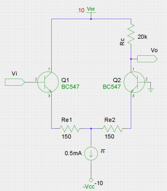
Now, consider a more complex example: A differential amplifier circuit.
 The schematic of the differential amplifier circuit is :
v 20110115 2
C 40000 40000 0 0 0 title-B.sym
C 46400 44400 1 0 0 resistor-1.sym
{
T 46700 44800 5 10 0 0 0 0 1
device=RESISTOR
T 46600 44700 5 10 1 1 0 0 1
refdes=Re1
T 46600 44200 5 10 1 1 0 0 1
value=150
}
C 47700 44400 1 0 0 resistor-1.sym
{
T 48000 44800 5 10 0 0 0 0 1
device=RESISTOR
T 47900 44700 5 10 1 1 0 0 1
refdes=Re2
T 47900 44200 5 10 1 1 0 0 1
value=150
}
C 48800 46900 1 90 0 resistor-1.sym
{
T 48400 47200 5 10 0 0 90 0 1
device=RESISTOR
T 48500 47000 5 10 1 1 90 0 1
refdes=Rc
T 48900 47200 5 10 1 1 0 0 1
value=20k
}
C 47300 44200 1 270 0 current-1.sym
{
T 48300 43600 5 10 0 0 270 0 1
device=CURRENT_SOURCE
T 47800 43900 5 10 1 1 270 0 1
refdes=Ic
T 46700 43700 5 10 1 1 0 0 1
value=0.5mA
}
C 45700 45400 1 0 0 BC547-1.sym
{
T 46600 46100 5 10 0 0 0 0 1
device=BC547
T 46600 45900 5 10 1 1 0 0 1
refdes=Q1
T 46500 45500 5 10 0 0 0 0 1
footprint=TO92
}
C 49300 45400 1 0 1 BC547-1.sym
{
T 48400 46100 5 10 0 0 0 6 1
device=BC547
T 48400 45900 5 10 1 1 0 6 1
refdes=Q2
T 48500 45500 5 10 0 0 0 6 1
footprint=TO92
}
C 47300 47800 1 0 0 vcc-1.sym
{
T 47100 48000 5 10 1 1 0 0 1
value=10
}
C 47200 42700 1 0 0 vcc-minus-1.sym
{
T 47600 42800 5 10 1 1 0 0 1
value=-10
}
N 46300 47800 46300 46400 4
N 46300 45400 46300 44500 4
N 46300 44500 46400 44500 4
N 47300 44500 47700 44500 4
N 48600 44500 48700 44500 4
N 48700 44500 48700 45400 4
N 47500 44200 47500 44500 4
N 48700 46900 48700 46400 4
C 49200 45600 1 0 0 gnd-1.sym
C 44900 45800 1 0 0 input-1.sym
{
T 44900 46100 5 10 0 0 0 0 1
device=INPUT
T 45100 46100 5 10 1 1 0 0 1
pinlabel=Vi
}
C 48700 46500 1 0 0 output-1.sym
{
T 48800 46800 5 10 0 0 0 0 1
device=OUTPUT
T 49300 46800 5 10 1 1 0 0 1
pinlabel=Vo
}
N 46300 47800 48700 47800 4
Following the process for parsing schematic, the first step is
- Identifying the components: After identifying the components and the attributes of components. The draft netlist without any placement yet is as below:
//Netlist_part1
module diffamp() begin;
RESISTOR #(.value(150)) Re1 (.p1(node1_1),.p2(node1_2));
RESISTOR #(.value(150)) Re2 (.p1(node2_1),.p2(node2_2));
RESISTOR #(.value(20k)) Rc  (.p1(node3_1),.p2(node3_2));
CURRENT_SOURCE #(.value(0.5mA)) Ic (.p1(node4_1),.p2(node4_2));
BC547 #(.footprint(TO92)) Q1 (.p1(node5_1),.p2(node5_2),.p3(node5_3));
BC547 #(.footprint(TO92)) Q2 (.p1(node6_1),.p2(node6_2),.p3(node6_3));
Vcc #(.value(10)) Vcc1 (.p1(node7_1));
-Vcc #(.value(-10)) Vcc2 (.p1(node8_1));
GND (.p1(node9_1));
INPUT Vi (.p1(node10_1));
OUTPUT Vo (.p1(node11_1));
//To_Add_Placement_and_Nets
endmodule
- Geting the absolute positions of the active edges of pins of the components, and place nodes which correspond to that pin of the component at that position in an `ifdef SCHEMATIC. The netlist after getting placement of nodes is :
//Netlist_part2
module diffamp() begin;
RESISTOR #(.value(150)) Re1 (.p1(node1_1),.p2(node1_2));
RESISTOR #(.value(150)) Re2 (.p1(node2_1),.p2(node2_2));
RESISTOR #(.value(20k)) Rc  (.p1(node3_1),.p2(node3_2));
CURRENT_SOURCE #(.value(0.5mA)) Ic (.p1(node4_1),.p2(node4_2));
BC547 #(.footprint(TO92)) Q1 (.p1(node5_1),.p2(node5_2),.p3(node5_3));
BC547 #(.footprint(TO92)) Q2 (.p1(node6_1),.p2(node6_2),.p3(node6_3));
Vcc #(.value(10)) Vcc1 (.p1(node7_1));
-Vcc #(.value(-10)) Vcc2 (.p1(node8_1));
GND (.p1(node9_1));
INPUT Vi (.p1(node10_1));
OUTPUT Vo (.p1(node11_1));
`ifdef SCHEMATIC
place #(.x(47300),.y(44500)) node1_1;
place #(.x(46400),.y(44500)) node1_2;
place #(.x(48600),.y(44500)) node2_1;
place #(.x(47700),.y(44500)) node2_2;
place #(.x(48700),.y(47800)) node3_1;
place #(.x(48700),.y(46900)) node3_2;
place #(.x(47500),.y(44200)) node4_1;
place #(.x(47500),.y(43300)) node4_2;
place #(.x(46300),.y(46400)) node5_1;
place #(.x(46300),.y(45400)) node5_2;
place #(.x(45700),.y(45900)) node5_3;
place #(.x(48700),.y(46400)) node6_1;
place #(.x(48700),.y(45400)) node6_2;
place #(.x(49300),.y(45900)) node6_3;
place #(.x(47500),.y(47800)) node7_1;
place #(.x(47500),.y(43300)) node8_1;
place #(.x(49300),.y(45900)) node9_1;
place #(.x(45700),.y(45900)) node10_1;
place #(.x(48700),.y(46600)) node11_1;
`endif
- Now in this step we search for 'net's in the schematic and write them. After writing nets, the final netlist is as follows.
//Netlist_part3_final
module diffamp() begin;
RESISTOR #(.value(150)) Re1 (.p1(node1_1),.p2(node1_2));
RESISTOR #(.value(150)) Re2 (.p1(node2_1),.p2(node2_2));
RESISTOR #(.value(20k)) Rc  (.p1(node3_1),.p2(node3_2));
CURRENT_SOURCE #(.value(0.5mA)) Ic (.p1(node4_1),.p2(node4_2));
BC547 #(.footprint(TO92)) Q1 (.p1(node5_1),.p2(node5_2),.p3(node5_3));
BC547 #(.footprint(TO92)) Q2 (.p1(node6_1),.p2(node6_2),.p3(node6_3));
Vcc #(.value(10)) Vcc1 (.p1(node7_1));
-Vcc #(.value(-10)) Vcc2 (.p1(node8_1));
GND (.p1(node9_1));
INPUT Vi (.p1(node10_1));
OUTPUT Vo (.p1(node11_1));

net net1 (node0  ,node5_1);
net net2 (node5_2,node1  );
net net3 (node1  ,node1_2);
net net4 (node1_1,node2_2);
net net5 (node2_1,node2  );
net net6 (node2  ,node6_2);
net net7 (node4_1,node3  );
net net8 (node3_2,node6_1);
net net9 (node0  ,node3_1);
net net10(node4_2,node8_1);
net net11(node5_3,node10_1);
net net12(node6_3,node9_1);
net net13(node3  ,node1_1);
net net14(node11_1,node3_2);
net net15(node7_1 ,node0  );

`ifdef SCHEMATIC
place #(.x(47300),.y(44500)) node1_1;
place #(.x(46400),.y(44500)) node1_2;
place #(.x(48600),.y(44500)) node2_1;
place #(.x(47700),.y(44500)) node2_2;
place #(.x(48700),.y(47800)) node3_1;
place #(.x(48700),.y(46900)) node3_2;
place #(.x(47500),.y(44200)) node4_1;
place #(.x(47500),.y(43300)) node4_2;
place #(.x(46300),.y(46400)) node5_1;
place #(.x(46300),.y(45400)) node5_2;
place #(.x(45700),.y(45900)) node5_3;
place #(.x(48700),.y(46400)) node6_1;
place #(.x(48700),.y(45400)) node6_2;
place #(.x(49300),.y(45900)) node6_3;
place #(.x(47500),.y(47800)) node7_1;
place #(.x(47500),.y(43300)) node8_1;
place #(.x(49300),.y(45900)) node9_1;
place #(.x(45700),.y(45900)) node10_1;
place #(.x(48700),.y(46600)) node11_1;
place #(.x(46300),.y(47800)) node0;
place #(.x(46300),.y(44500)) node1;
place #(.x(48700),.y(44500)) node2;
place #(.x(47500),.y(44500)) node3;
`endif
How to build schematics
The following procedure outlines how a schematic is built from a verilog netlist. This constitutes the second part of the proposal [1]. It is mostly the inverse of parsing schematics.
Create an augmented netlist with placement info
- Get the symbols to be used for each component(module in the netlist) with help of user input
- User gives the symbol to use directly
- User gives the symbol name from the standard library which can be obtained
- User gives the 'device' attribute that corresponds to that module which can be searched from the standard symbols
- Replace the modules of original netlist with new modules named with the 'device' name. They are same as the original modules but with a parameter string 'sym' which corresponds to the symbol to be used for that device.
- Rename the nodes connected to pins of the components such that each has unique name and separate the collapsed nets and place a net between such nodes with default (ideal) parameters i.e, 'zero' resistance, 'zero' inductance etc.
- Place the nodes in an `ifdef directive using 'place' module which takes 2 attributes x,y ,the co-ordinates of the node. (*TODO : heuristic for placement)
Position the components in the schematic
- Place components in between the nodes their pins are connected. In case of a 2-pin device place the pins in between the nodes. Get the device position using relative positions of pins in a symbol.
- Write the first line in gschem file with appropriate version (not needed but better done) and place the components at the positions calculated above
- Add text attributes to the components in schematic like device, refdes, value etc. Use the format T xc yc 5 10 0 0 0 0 1 for invisible attributes like device. Use T xc yc 5 10 1 1 0 0 1 for value-only visible attributes. Refer to [4] for specs
Creating nets between nodes and pins
- Write nets from the nodes to the pins they connect.
- Look for 'net's in the netlist and write a net from the co-ordinates of one node to another connected node.
- (*TODO): In case a net is slant, to use complex connection between pins made of horizontal/vertical nets.
Example of Building
Consider the voltage divider circuit netlist as written below.
module voltage_div ();
//A simple voltage divider circuit as an example
resistor #(.r(2k)) R1  (.p(p1),.n(p2));
resistor #(.r(1k)) R2  (.p(p2),.n(p3));
vsource #(.dc(10)) Vin (.p(p1),.n(p3));
endmodule
- With the help of user input, we now get the symbols that we use for each module. For resistor we use resistor-1.sym. It will be determined in either of following ways
- User gives the symbol to use directly (wrote by them)
- User gives the symbol name from the standard library which can be obtained
- User gives the 'device' attribute for the component and we can search the standard library or a built-index (?) of it for symbols with such a device name
- Now we create an augmented netlist from this with the placement info and different modules defined by the name same as the value of 'device' attribute (eg. RESISTOR etc).
- If the nets are collapsed between pins/nodes, then separate them and place a net in between the nodes with parameter values of the net 'zero' (resistance,inductance etc) i.e, the ideal connection
- Place the nodes of components at some place. For now they'll be placed randomly. Random placement gives unaesthetic schematics. (*TODO) Develop a heuristic so that placement is not random and has aesthetic appeal.
The augmented netlist is
//augmented_netlist_with_placement
module voltage_div ();
RESISTOR #(.r(2k),.sym(resistor-1.sym) R1  (.p(node11),.n(node12));
RESISTOR #(.r(1k),.sym(resistor-1.sym)) R2  (.p(node21),.n(node22));
VOLTAGE_SOURCE #(.dc(10),.sym(voltage-3.sym)) Vin (.p(node31),.p(node32));
net net1 (node12,node21); //this net is corresponds to net at pin p2
net net2 (node22,node32); //corresponds to net at pin p3
net net3 (node11,node31); //corresponds to net at pin p1
`ifdef SCHEMATIC //placing the nodes randomly as multiples of 100
//,not differing by too much and taking care that nodes of same device differ only in one of the x & y co-ordinated
  place #(.x(45200),.y(48100)) node11;
  place #(.x(43900),.y(48100)) node12;
  place #(.x(43800),.y(47000)) node21;
  place #(.x(42800),.y(47000)) node22;
  place #(.x(43800),.y(46400)) node31;
  place #(.x(43800),.y(47400)) node32;
`endif
endmodule

module RESISTOR(pin1,pin2) begin;
parameter string sym;
parameter real res;
electrical pin1,pin2;
resistor #(.r(res)) R (.p(pin1),.n(pin2));
endmodule

module VOLTAGE_SOURCE(pinp,pinn) begin;
parameter string sym;
parameter real dc;
electrical pinp,pinn;
vsource #(.dc(dc)) Vs (.p(pinp),.n(pinn));
endmodule
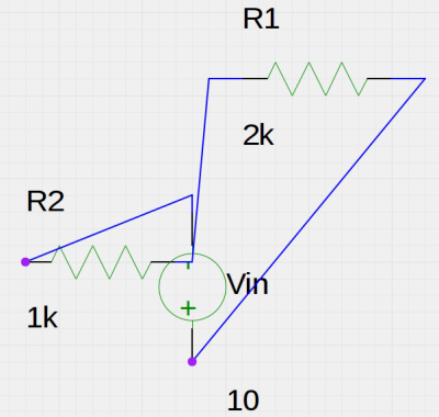
- Now, we start building the schematic from the augmented netlist. First, we write the nets connecting nodes. 'net's in verilog connect 2 nodes. As all nodes have been placed in the 'ifdef directive, we can write nets in schematic as follows.
- Write the version line in the start and write nets starting with the identifier 'N' followed by the x & y co-ordinates of the nodes the net connects.
v 20100214 2
//components yet to be placed.
N 43900 48100 43800 47000 5 //net1
N 42800 47000 43800 47400 5 //net2
N 45200 48100 43800 46400 5 //net3
- Now, we place the components in between the nodes their pins are connected to. Resistor R1 is connected between node11 and node 12. We get device position as follows :
node11=[45200,48100]
node12=[43900,48100]
for i in range(len(node11)):
  node_m[i]=(node11[i]+node12[i])/2
#that gives node_m=[44550,49000]
#the resistor has pins at
p1_abs=[0,100]
p2_abs=[900,100]
#So the pins' absolute positions are
for i in range(2):
  p12[i]=(p2_abs[i]-p1_abs[i])/2
  p1[i]=node_m[i]-p12[i] #p1=[44550-450,49000]=[41000,49000] and
  p2[i]=node_m[i]+p12[i] #p2=[44550+450,49000]=[45000,49000]
  dev[i]=p1[i]-p1_abs[i] #The device is the placed at 'p1'-'p1_abs'
#this logic needs to be improved..
- Now we get all pin positions and device positions from the above logic.
p11: (45200,48100) ; p12: (44100,48100) ; //device R1
p21: (43700,47000) ; p22: (42800,47000) ; //device R2
p31: (43800,46400) ; p32: (43800,47300) ; //device Vin
R1 : (44100,48000) ; R2 : (42800,46900) ; Vin: (44000,46400) and rotated by 90.
- Using the placement of pins and components from above logic. We position the components and connect the pins to the nodes through nets.
v 20100214 2
C 44100 48000 1 0 0 resistor-1.sym
{
T 44100 48000 5 10 0 0 0 0 1
device=RESISTOR
T 44100 48400 5 10 1 1 0 0 1
refdes=R1
T 44100 47700 5 10 1 1 0 0 1
value=2k
}
C 42800 46900 1 0 0 resistor-1.sym
{
T 42800 46900 5 10 0 0 0 0 1
device=RESISTOR
T 42800 47300 5 10 1 1 0 0 1
refdes=R2
T 42800 46600 5 10 1 1 0 0 1
value=1k
}
C 44000 46400 1 90 0 voltage-3.sym
{
T 44000 46400 5 10 0 0 0 0 1
device=VOLTAGE_SOURCE
T 44000 46800 5 10 1 1 0 0 1
refdes=Vin
T 44000 46100 5 10 1 1 0 0 1
value=10
}

N 45200 48100 45000 48100 4 //p11
N 43900 48100 44100 48100 4 //p12
N 43800 47000 43700 47000 4 //p21
N 42800 47000 42800 47000 4 //p22
N 43800 46400 43800 46400 4 //p31
N 43800 47400 43800 47300 4 //p32

N 43900 48100 43800 47000 4 //net1
N 42800 47000 43800 47400 4 //net2
N 45200 48100 43800 46400 4 //net3
References
[1] GSoC Proposal
[2] gEDA/gschem
[3] Schematic Attribute List : graphical
[4] File format specs : Schematic
[5] Blog contains weekly updates and documentation of the timeline for this project under GSoC.
[6] Github branch containing the old code.
[7] newer code
